- 您现在的位置:买卖IC网 > Sheet目录337 > LT3466EDD-1#PBF (Linear Technology)IC LED DRIVR WHITE BCKLGT 10-DFN
�� �
�
�LT3466-1�
�OPERATIO�
�Main� Control� Loop�
�The� LT3466-1� uses� a� constant� frequency,� current� mode�
�control� scheme� to� provide� excellent� line� and� load� regula-�
�tion.� It� incorporates� two� similar,� but� fully� independent� PWM�
�converters.� Operation� can� be� best� understood� by� referring�
�to� the� Block� Diagram� in� Figure� 2.� The� oscillator,� start-up�
�bias� and� the� bandgap� reference� are� shared� between� the�
�two� converters.� The� control� circuitry,� power� switch,� Schot-�
�tky� diode� etc.,� are� similar� for� both� converters.�
�At� power-up,� the� output� voltages� V� OUT1� and� V� OUT2� are�
�charged� up� to� V� IN� (input� supply� voltage)� via� their� respec-�
�tive� inductor� and� the� internal� Schottky� diode.� If� either�
�CTRL1� and� CTRL2� or� both� are� pulled� high,� the� bandgap�
�reference,� start-up� bias� and� the� oscillator� are� turned� on.�
�Working� of� the� main� control� loop� can� be� understood� by�
�following� the� operation� of� converter� 1.� At� the� start� of� each�
�oscillator� cycle,� the� power� switch� Q1� is� turned� on.� A�
�voltage� proportional� to� the� switch� current� is� added� to� a�
�stabilizing� ramp� and� the� resulting� sum� is� fed� into� the�
�positive� terminal� of� the� PWM� comparator� A2.� When� this�
�voltage� exceeds� the� level� at� the� negative� input� of� A2,� the�
�PWM� logic� turns� off� the� power� switch.� The� level� at� the�
�negative� input� of� A2� is� set� by� the� error� amplifier� A1,� and� is�
�simply� an� amplified� version� of� the� difference� between� the�
�feedback� voltage� and� the� 200mV� reference� voltage.� In� this�
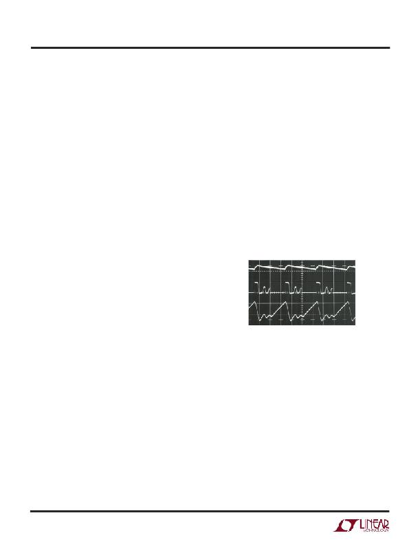
�Minimum� Output� Current�
�The� LT3466-1� can� drive� a� 6-LED� string� at� 3mA� LED� current�
�without� pulse� skipping.� As� current� is� further� reduced,� the�
�device� may� begin� skipping� pulses.� This� will� result� in� some�
�low� frequency� ripple,� although� the� LED� current� remains�
�regulated� on� an� average� basis� down� to� zero.� The� photo� in�
�Figure� 3� shows� circuit� operation� with� 6� white� LEDs� at� 3mA�
�current� driven� from� 3.6V� supply.� Peak� inductor� current� is�
�less� than� 50mA� and� the� regulator� operates� in� discontinu-�
�ous� mode� implying� that� the� inductor� current� reached� zero�
�during� the� discharge� phase.� After� the� inductor� current�
�reaches� zero,� the� switch� pin� exhibits� ringing� due� to� the� LC�
�tank� circuit� formed� by� the� inductor� in� combination� with�
�switch� and� diode� capacitance.� This� ringing� is� not� harmful;�
�far� less� spectral� energy� is� contained� in� the� ringing� than� in�
�the� switch� transitions.� The� ringing� can� be� damped� by�
�application� of� a� 300� ?� resistor� across� the� inductors,� al-�
�though� this� will� degrade� efficiency.�
�V� OUT1�
�20mV/DIV�
�(AC-COUPLED)�
�V� SW1�
�20V/DIV�
�I� L1�
�50mA/DIV�
�manner,� the� error� amplifier� A1� regulates� the� voltage� at� the�
�FB1� pin� to� 200mV.� The� output� of� the� error� amplifier� A1� sets�
�V� IN� =� 3.6V� 0.5� μ� s/DIV�
�I� LED1� =� 3mA�
�CIRCUIT� OF� FIGURE� 1�
�34661� F03�
�the� correct� peak� current� level� in� inductor� L1� to� keep� the�
�output� in� regulation.� The� CTRL1� pin� voltage� is� used� to�
�adjust� the� feedback� voltage.�
�The� working� of� converter� 2� is� similar� to� converter� 1� with�
�the� exception� that� the� feedback� 2� reference� voltage� is�
�800mV.� The� error� amplifier� A1� in� converter� 2� regulates� the�
�voltage� at� the� FB2� pin� to� 800mV.� If� only� one� of� the�
�converters� is� turned� on,� the� other� converter� will� stay� off�
�and� its� output� will� remain� charged� up� to� V� IN� (input� supply�
�voltage).� The� LT3466-1� enters� into� shutdown,� when� both�
�CTRL1� and� CTRL2� are� pulled� lower� than� 70mV.� The� CTRL1�
�and� CTRL2� pins� perform� independent� dimming� and� shut-�
�down� control� for� the� two� converters.�
�Figure� 3.� Switching� Waveforms�
�Overvoltage� Protection�
�The� LT3466-1� has� internal� overvoltage� protection� for� both�
�converters.� In� the� event� the� white� LEDs� are� disconnected�
�from� the� circuit� or� fail� open,� the� converter� 1� output� voltage�
�is� clamped� at� 39.5V� (typ).� Figure� 4(a)� shows� the� transient�
�response� of� the� circuit� in� Figure� 1� with� LED1� disconnected.�
�With� the� white� LEDs� disconnected,� the� converter� 1� starts�
�switching� at� the� peak� current� limit.� The� output� of� converter�
�1� starts� ramping� up� and� finally� gets� clamped� at� 39.5V� (typ).�
�The� converter� 1� will� then� switch� at� low� inductor� current� to�
�regulate� the� output� voltage.� Output� voltage� and� input�
�current� during� output� open� circuit� are� shown� in� the� Typical�
�Performance� Characteristics� graphs.�
�34661f�
�8�
�发布紧急采购,3分钟左右您将得到回复。
相关PDF资料
LT3466EDD#PBF
IC LED DRIVR WHITE BCKLGT 10-DFN
LT3474IFE#PBF
IC LED DRVR HP CONS CURR 16TSSOP
LT3475EFE-1#PBF
IC LED DRVR HP CONS CURR 20TSSOP
LT3476EUHF#PBF
IC LED DRVR HP CONST CURR 38-QFN
LT3477EFE#PBF
IC LED DRVR HP CONS CURR 20TSSOP
LT3478IFE#PBF
IC LED DRVR HP CONS CURR 16TSSOP
LT3486EFE#PBF
IC LED DRVR WHITE BCKLGT 16TSSOP
LT3491EDC#TRMPBF
IC LED DRIVER WHITE BCKLGT 6-DFN
相关代理商/技术参数
LT3466EDD-1#PBF
制造商:Linear Technology 功能描述:IC, LED DRVR, DFN10
LT3466EDD-1#TRPBF
功能描述:IC LED DRIVR WHITE BCKLGT 10-DFN RoHS:是 类别:集成电路 (IC) >> PMIC - LED 驱动器 系列:- 标准包装:6,000 系列:- 恒定电流:- 恒定电压:- 拓扑:开路漏极,PWM 输出数:4 内部驱动器:是 类型 - 主要:LED 闪烁器 类型 - 次要:- 频率:400kHz 电源电压:2.3 V ~ 5.5 V 输出电压:- 安装类型:表面贴装 封装/外壳:8-VFDFN 裸露焊盘 供应商设备封装:8-HVSON 包装:带卷 (TR) 工作温度:-40°C ~ 85°C 其它名称:935286881118PCA9553TK/02-TPCA9553TK/02-T-ND
LT3466EDDPBF
制造商:Linear Technology 功能描述:Dual Full Func White LED contrlr,LT3466
LT3466EFE
制造商:Linear Technology 功能描述:LED DRVR 20Segment 3.3V/5V/9V/12V/15V/18V 16-Pin TSSOP EP
LT3466EFE#PBF
功能描述:IC LED DRVR WHITE BCKLGT 16TSSOP RoHS:是 类别:集成电路 (IC) >> PMIC - LED 驱动器 系列:- 标准包装:60 系列:- 恒定电流:- 恒定电压:- 拓扑:线性(LDO),PWM,升压(升压) 输出数:8 内部驱动器:是 类型 - 主要:背光 类型 - 次要:RGB,白色 LED 频率:500kHz ~ 1.5MHz 电源电压:4.75 V ~ 26 V 输出电压:45V 安装类型:* 封装/外壳:* 供应商设备封装:* 包装:* 工作温度:-40°C ~ 85°C
LT3466EFE#TRPBF
功能描述:IC LED DRVR WHITE BCKLGT 16TSSOP RoHS:是 类别:集成电路 (IC) >> PMIC - LED 驱动器 系列:- 标准包装:6,000 系列:- 恒定电流:- 恒定电压:- 拓扑:开路漏极,PWM 输出数:4 内部驱动器:是 类型 - 主要:LED 闪烁器 类型 - 次要:- 频率:400kHz 电源电压:2.3 V ~ 5.5 V 输出电压:- 安装类型:表面贴装 封装/外壳:8-VFDFN 裸露焊盘 供应商设备封装:8-HVSON 包装:带卷 (TR) 工作温度:-40°C ~ 85°C 其它名称:935286881118PCA9553TK/02-TPCA9553TK/02-T-ND
LT3467
制造商:LINER 制造商全称:Linear Technology 功能描述:700mA Low Noise High Current LED Charge Pump
LT3467A
制造商:LINER 制造商全称:Linear Technology 功能描述:700mA Low Noise High Current LED Charge Pump